
SERIES SAR
High Voltage, Isolated, Adjustable Output Modules
100 to 1500 VDC at 3 W Output
Adjustable down to 0V Output
3 Standard Wide Input Voltages:
5SAR (5-10VDC)
12SAR (7.5-15VDC)
24SAR (18-36VDC)
Single Output with Center Tap
Low Profile DC-DC Converters
Thru Hole and Surface Mount
The SAR Series of Adjustable, Isolated, Single Output High Voltage ultra miniature DC-DC Converters are fully encapsulated for use in a harsh environment. The units in the SAR Series have high efficiency, excellent line/load regulation, and operate over a temperature range of -25°C to +70°C with no electrical de-rating or heat-sinking required.
FEATURES
DIMENSIONS: Thru Hole: 1.10" x 0.80" x 0.425" Typical (WxDxH) |
OPTIONS AVAILABLE :
OTHER CHARACTERISTICS: Input Voltage Nominal (Vin, Nom): 5VDC, 12VDC, 24VDC |
APPLICATIONS
|
|
|
|
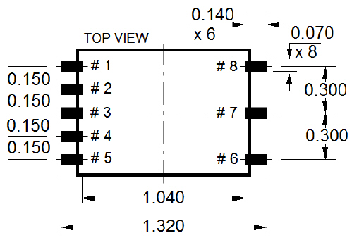
Thru Hole Models
|
||||||||||||||||||||
|
|
|
PIN DESCRIPTION PIN #1( -IN) and PIN #5 (+IN): Input Voltage to the unit. Unit features a wide input range in the ration of 2:1. Input is Over Voltage and Under Voltage protected with non-latching Shutdown. PIN #2 (ADJ): used for changing the Output Voltage in Resistor Programming or Voltage Programming mode. A resistor connected between Pin #2 (ADJ) and Pin #1 (-IN) will reduce Vout. A voltage applied across Pin #2 and Pin #1 between 0 and 3V will program Vout between 0 and Vout Max. PIN #3 (REF): Onboard Reference, 3V +/- 5% sourcing 1mA Max. A voltage divider connected between Pin #3 (REF) and Pin #1 (-IN) could be used for Output Voltage Programming PIN #4 (SHDN): Will shut down the output when pulled down to Pin #1 (-IN) PIN #6 (+OUT) and Pin #8 (-OUT): Output Pins PIN #7 (COM): Is a Center Tap between (+OUT) and (-OUT) and can be used as a common output pin for Dual Output Bipolar Operation. |
||||||||||||||||||

|
Surface Mount Models
|
||||||||||||||||||||
|
|
|
PIN DESCRIPTION PIN #1( -IN) and PIN #5 (+IN): Input Voltage to the unit. Unit features a wide input range in the ration of 2:1. Input is Over Voltage and Under Voltage protected with non-latching Shutdown. PIN #2 (ADJ): used for changing the Output Voltage in Resistor Programming or Voltage Programming mode. A resistor connected between Pin #2 (ADJ) and Pin #1 (-IN) will reduce Vout. A voltage applied across Pin #2 and Pin #1 between 0 and 3V will program Vout between 0 and Vout Max. PIN #3 (REF): Onboard Reference, 3V +/- 5% sourcing 1mA Max. A voltage divider connected between Pin #3 (REF) and Pin #1 (-IN) could be used for Output Voltage Programming PIN #4 (SHDN): Will shut down the output when pulled down to Pin #1 (-IN) PIN #6 (+OUT) and Pin #8 (-OUT): Output Pins PIN #7 (COM): Is a Center Tap between (+OUT) and (-OUT) and can be used as a common output pin for Dual Output Bipolar Operation. |
||||||||||||||||||

LAND PATTERN
All Dimensions are Typical and in Inches
| SERIES 5SAR (25°C ambient, Vi, nom and Pout, Max.) |
||||||||||||||||
|---|---|---|---|---|---|---|---|---|---|---|---|---|---|---|---|---|
| PICO PART # | INPUT VOLTAGE | OUTPUT VOLTAGE | INPUT CURRENT | MAX. OUTPUT CURRENT (mA) | * MAX. OUTPUT POWER (W) |
LINE REG. (%) | ** LOAD REG. (%) |
EFF. (%) | *** OUTPUT RIPPLE (%) |
PRICE (US $) | ||||||
| Thru Hole | Surface Mount | VI Nom (VDC) |
RANGE (VDC) |
RANGE (VDC) |
SETUP TOL (±%) | NO LOAD (mA) | FULL LOAD (mA) | |||||||||
| MIN | MAX | MIN | MAX | |||||||||||||
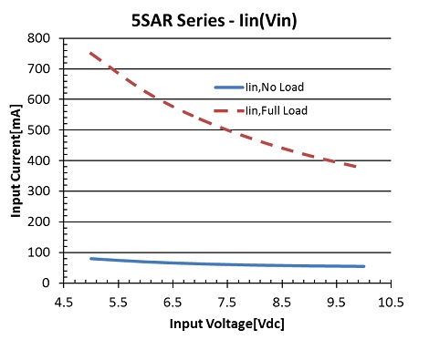
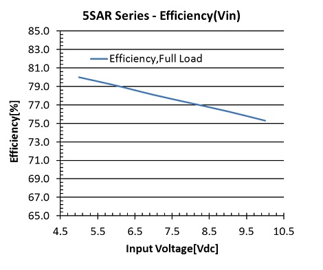
| 5SAR100 | 5SAR100SM | 7.5 | 5 | 10 | 0 | 100 | 3 | 45 | 510 | 30 | 3 | 0.1 | 8 | 78 | 0.2 | 171.55 |
| 5SAR250 | 5SAR250SM | 7.5 | 5 | 10 | 0 | 250 | 3 | 56 | 512 | 12 | 3 | 0.1 | 5 | 78 | 0.15 | 197.96 |
| 5SAR500 | 5SAR500SM | 7.5 | 5 | 10 | 0 | 500 | 3 | 76 | 517 | 6 | 3 | 0.1 | 4 | 77 | 0.15 | 211.94 |
| 5SAR1000 | 5SAR1000SM | 7.5 | 5 | 10 | 0 | 1000 | 3 | 76 | 530 | 3 | 3 | 0.1 | 5 | 75 | 0.2 | 247.44 |
| 5SAR1500 | 5SAR1500SM | 7.5 | 5 | 10 | 0 | 1500 | 3 | 71 | 546 | 2 | 3 | 0.1 | 5 | 74 | 0.3 | 289.07 |
| NOTES: * See Max Power De-rating Diagram ** Load Regulation measured between No Load and Full Load *** Output Ripple measured with 1MHz Bandwidth |
||||||||||||||||
|
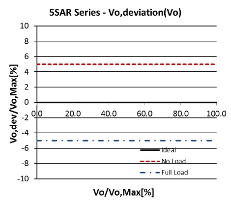
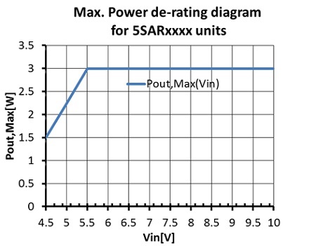
5SAR SERIES DIAGRAMS
|
|
|
|
|
|
|
|
 |
|---|
| SERIES 12SAR (25°C ambient, Vi, nom and Pout, Max.) |
||||||||||||||||
|---|---|---|---|---|---|---|---|---|---|---|---|---|---|---|---|---|
| PICO PART # | INPUT VOLTAGE | OUTPUT VOLTAGE | INPUT CURRENT | MAX. OUT CUR (mA) | MAX. OUT POW (W) | LINE REG. (%) | * LOAD REG. (%) |
EFF. (%) | ** OUTPUT RIPPLE (%) |
PRICE (US $) | ||||||
| Thru Hole | Surface Mount | VI Nom (VDC) |
RANGE (VDC) |
RANGE (VDC) |
SETUP TOL (±%) | NO LOAD (mA) | FULL LOAD (mA) | |||||||||
| MIN | MAX | MIN | MAX | |||||||||||||
| 12SAR100 | 12SAR100SM | 12 | 7.5 | 15 | 0 | 100 | 3 | 55 | 310 | 30 | 3 | 0.1 | 5 | 80 | 0.2 | 171.55 |
| 12SAR250 | 12SAR250SM | 12 | 7.5 | 15 | 0 | 250 | 3 | 56 | 309 | 12 | 3 | 0.1 | 3 | 81 | 0.15 | 197.96 |
| 12SAR500 | 12SAR500SM | 12 | 7.5 | 15 | 0 | 500 | 3 | 44 | 315 | 6 | 3 | 0.1 | 4 | 79 | 0.4 | 211.94 |
| 12SAR1000 | 12SAR1000SM | 12 | 7.5 | 15 | 0 | 1000 | 3 | 50 | 320 | 3 | 3 | 0.1 | 4 | 79 | 0.25 | 247.44 |
| 12SAR1500 | 12SAR1500SM | 12 | 7.5 | 15 | 0 | 1500 | 3 | 51 | 318 | 2 | 3 | 0.1 | 4 | 78 | 0.3 | 289.07 |
| NOTES: * Load Regulation measured between No Load and Full Load ** Output Ripple measured with 1MHz Bandwidth |
||||||||||||||||
|
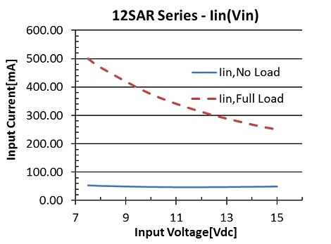
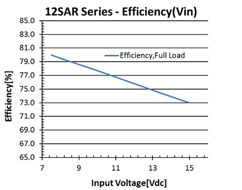
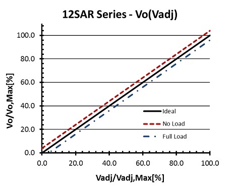
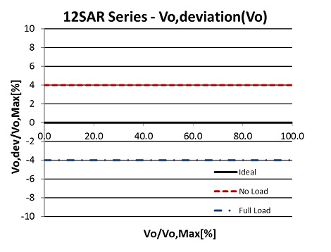
12SAR DIAGRAMS
|
|
|
|
|
|
|
|
| SERIES 24SAR (25°C ambient, Vi, nom and Pout, Max.) |
||||||||||||||||
|---|---|---|---|---|---|---|---|---|---|---|---|---|---|---|---|---|
| PICO PART # | INPUT VOLTAGE | OUTPUT VOLTAGE | INPUT CURRENT | MAX. OUT CUR (mA) | MAX. OUT POW (W) | LINE REG. (%) | * LOAD REG. (%) |
EFF. (%) | ** OUTPUT RIPPLE (%) |
PRICE (US $) | ||||||
| Thru Hole | Surface Mount | VI Nom (VDC) |
RANGE (VDC) |
RANGE (VDC) |
SETUP TOL (±%) | NO LOAD (mA) | FULL LOAD (mA) | |||||||||
| MIN | MAX | MIN | MAX | |||||||||||||
| 24SAR100 | 24SAR100SM | 24 | 18 | 36 | 0 | 100 | 3 | 35 | 168 | 30 | 3 | 0.5 | 5 | 75 | 0.35 | 171.55 |
| 24SAR250 | 24SAR250SM | 24 | 18 | 36 | 0 | 250 | 3 | 32 | 165 | 12 | 3 | 0.5 | 3 | 75 | 0.3 | 197.96 |
| 24SAR500 | 24SAR500SM | 24 | 18 | 36 | 0 | 500 | 3 | 29 | 165 | 6 | 3 | 0.5 | 4 | 77 | 0.2 | 211.94 |
| 24SAR1000 | 24SAR1000SM | 24 | 18 | 36 | 0 | 1000 | 3 | 30 | 167 | 3 | 3 | 0.5 | 4 | 76 | 0.2 | 247.44 |
| 24SAR1500 | 24SAR1500SM | 24 | 18 | 36 | 0 | 1500 | 3 | 39 | 170 | 2 | 3 | 0.5 | 4 | 73 | 0.2 | 289.07 |
| NOTES: * Load Regulation measured between No Load and Full Load ** Output Ripple measured with 1MHz Bandwidth |
||||||||||||||||
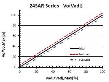
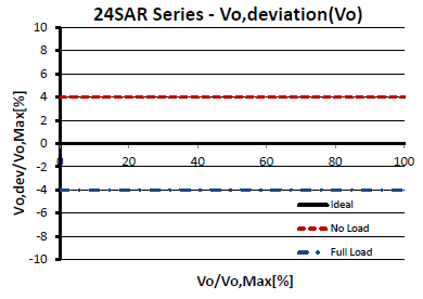
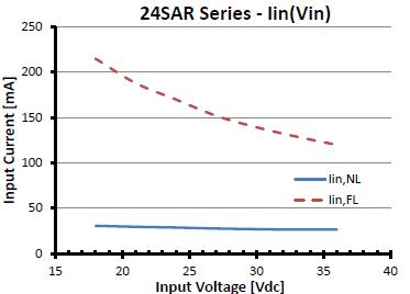
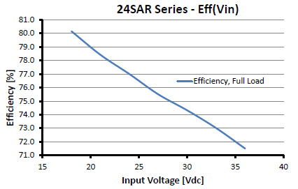
| 24SAR DIAGRAMS | |
|---|---|
 |
 |
 |
 |
 |
|---|
|
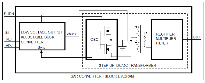
The SAR Series of DC-DC High Voltage Converters is based on a two stage design. The first stage is a low voltage Buck Converter that produces a regulated and adjustable voltage (Vbuck) to be stepped-up by the second stage; a fixed step-up ratio DC-DC transformer. The DC-DC transformers consists of a Push-Pull oscillator, synchronized at half the buck frequency, a step-up transformer, followed by a rectifier/multiplier and a filter circuit. It has no active regulation circuit. However, due to a resonant design, it exhibits a very low load effect. A high impedance programming input (Vadj) controls the Buck Conerter output and allows for 0V to maximum voltage adjustment. The Buck Converter features excellent line regulation an any Vadj level and over the entire input range. Overal, the SAR Series will provide 0V to Max. HV adjustability with tight input regulation across the input range and a minimal load effect. The following are designed in functions that increase module versatility:
|
| INPUT UNDER/OVER VOLTAGE SHUTDOWN | |||
|---|---|---|---|
| Unit | 5SAR Series | 12SAR Series | 24SAR Series |
| UV SHDN (V) | 4 | 7 | 16 |
| OV SHDN (V) | 10.5 | 16 | 38 |
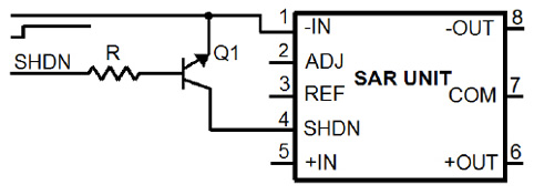
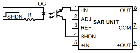
REMOTE SHUTDOWN: The converter is turned off when Pin #4 (SHDN) is clamped to Pin #1 (-IN) within less than 0.4V.
|
NON-ISOLATED SHUTDOWN |
ISOLATED SHUTDOWN |
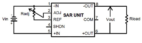
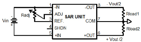
SINGLE/DUAL OUTPUT OPERATION: The converter can be operated as a single output source of nominal Vout with a load connected between (-Out) and (+Out) or as a dual bipolar source with loads connected between (-Out) and (Com) AND (+Out) and (Com) respectively with each load being powered at Vout/2.
|
SINGLE OUTPUT |
DUAL OUTPUT - BIPOLAR |
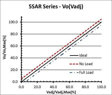
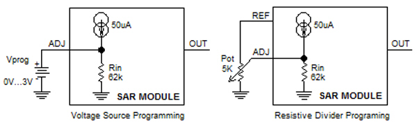
OUTPUT PROGRAMMING: At power-up and with ADJ pin not connected, the SAR Output will be at maximum voltage.
RESISTOR PROGRAMMING:
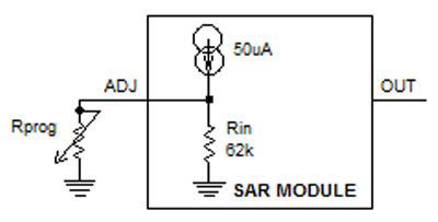 |
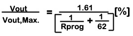
A resistor connected from ADJ pin to ground will decrease the output voltage. The following formula shows, with reasonable accuracy, the relation between Vout and Rprog, where Rprog is in kohm:
For instance, to adjust to 25% Vout,Max., Rprog is 21kohm, for 50% is 62kohm, and for 75% it is 187kohm. NOTE: Resistor Programming in not available for 24SAR Modules |
|---|
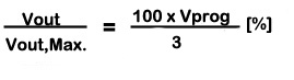
VOLTAGE PROGRAMMING:
 |
|---|
|
A voltage source to ADJ pin will program the output voltage linearly. 0V ADJ corresponds to 0V OUT and 3V ADJ corresponds to Vout,Max. The following formula applies: The REF output is useful for programming purposes. A resistor divider or potentiometer could make the circuit for voltage adjustment. In order to keep programming error low, it is recommended for the overall resistance of the divider to not exceed 5kohm. |
For immediate engineering assistance or to place an order:
Call Toll Free: 800-431-1064
PICO Electronics, Inc.
143 Sparks Ave. Pelham, NY 10803-1810
Tel: 914-738-1400 or Fax: 914-738-8225